India’s push to build a strong domestic semiconductor design ecosystem is showing signs of growing momentum, with companies supported under the government’s Design Linked Incentive (DLI) scheme collectively raising more than $100 million in venture capital and completing 35 chip-design tape-outs.
The progress reflects a shift from early-stage chip development towards products that have reached important validation milestones and are moving closer to commercialisation.
Aheesa’s VIHAAN Chip Clears First Silicon Test
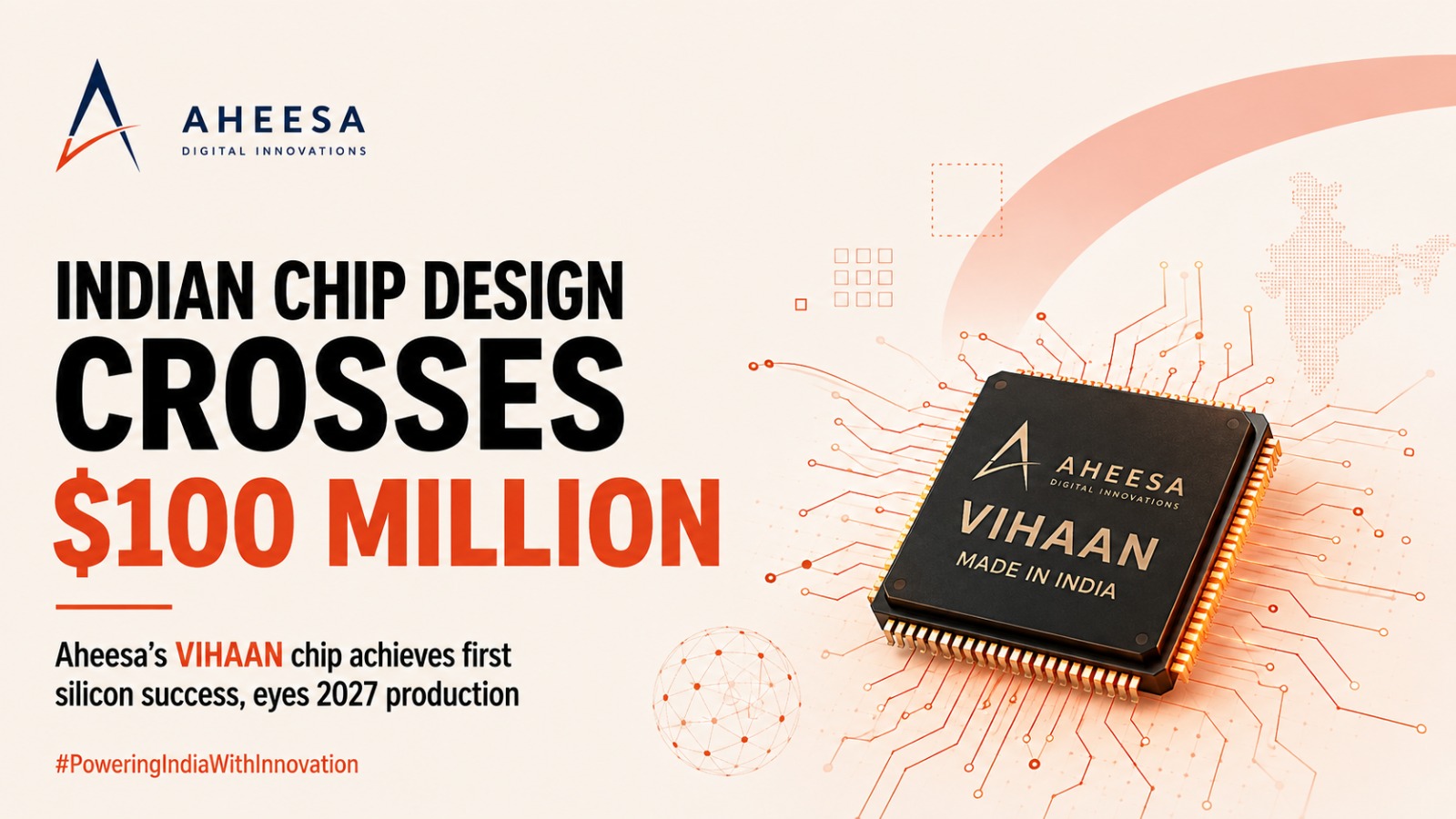
One of the latest milestones has come from Chennai-based fabless semiconductor startup Aheesa Digital Innovations. Its VIHAAN networking System-on-Chip achieved first-pass silicon success on Independence Day after the chip was taped out on Republic Day earlier this year.
The chip has been developed for fibre broadband networking. Following the successful first silicon, Aheesa is expected to move towards a production tape-out targeted for 2027.
In semiconductor development, a tape-out is the stage at which a completed chip design is sent to a fabrication facility for manufacturing. First-pass silicon success means the fabricated chip performs as intended in its first iteration, making it an important milestone before a product progresses towards commercial production.
Aheesa develops semiconductor solutions for broadband networking and security. Earlier this year, the company raised around Rs 40 crore from the Tamil Nadu Infrastructure Fund Management Corporation (TNIFMC) through the Tamil Nadu Emerging Sector Seed Fund, along with other private investors.
The funding highlights the growing investor interest in domestic semiconductor design ventures supported through the DLI programme.
Also Read: Meet NeoSapien: The Bengaluru Startup Building an AI ‘Second Brain’
DLI Expands Support Across Multiple Industries
The Design Linked Incentive scheme supports startups working on semiconductor designs for a wide range of applications. These include satellite communications, drones, defence systems, automobiles, Internet of Things devices, artificial intelligence, telecom equipment, surveillance cameras and smart meters.
The government has also expanded access to infrastructure needed for chip development. Advanced chip-design tools have been made available to 455 organisations, comprising 350 academic institutions and 105 startups.
Alongside the DLI initiative, the Chips to Startup programme is helping build the next generation of semiconductor talent. Under the programme, 71 academic institutions have completed 245 chip-design tape-outs.
More Indian Chip Startups Reach Key Milestones
Several other companies backed under the DLI framework have also reported important developments in recent months.
Vervesemi Microelectronics has achieved first-pass silicon success for a BLDC motor-controller chip that uses an indigenous processor developed by Incore Semiconductor.
Netrasemi has tested a 12nm Vision SoC featuring integrated acceleration for video analytics. OptoML, meanwhile, has received its 12nm compute-in-memory SoC, which is designed to support faster and more power-efficient artificial intelligence processing.
Mindgrove Technologies has partnered with PRAMA India to explore the use of its Vision SoC in CCTV cameras. IndieSemiC has also secured global certification for its Bluetooth Low Energy 6 chip module, marking another step towards wider deployment of Indian-designed semiconductor technology.
Chip Design Holds High Value in Electronics
Chip design remains one of the highest-value segments of the semiconductor industry. It can contribute up to half of the overall value addition in the semiconductor chain and accounts for around 15% to 35% of the bill-of-materials cost of electronic products.
For India, developing domestic design capabilities is therefore an important part of building a broader semiconductor ecosystem. The growing number of tape-outs and successful silicon validations indicates that more locally designed chips are progressing beyond the development stage.
Semicon 2.0 Broadens India’s Semiconductor Ambition
The developments come as the government expands its semiconductor programme through Semicon 2.0, which was approved in July with an outlay of Rs 1.27 lakh crore.
The wider programme aims to strengthen capabilities across semiconductor design, fabrication, packaging, equipment, materials, research and development, and skilled manpower.
With more Indian chip companies now reaching tape-out and silicon-validation milestones, the next major challenge will be taking these designs into volume manufacturing and securing global supply contracts. The ability to make that transition will be crucial to turning India’s growing semiconductor design capabilities into a larger and more competitive domestic industry.
Also Read: Meet FutureSports: The Startup Bringing Wall Street Mechanics to the