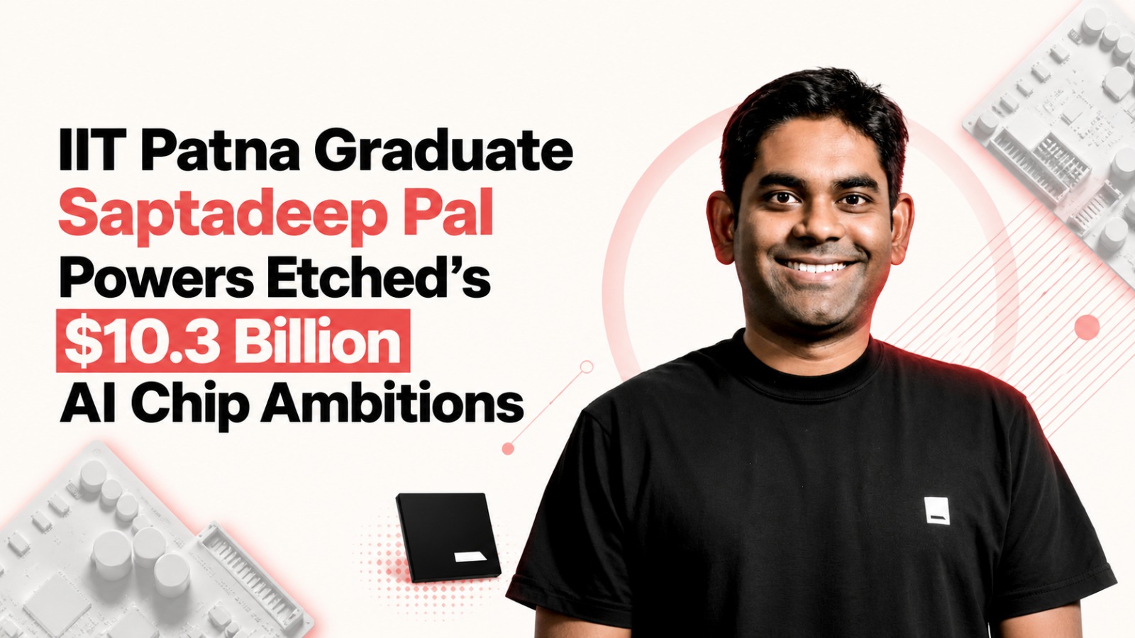
Artificial intelligence chip startup Etched has emerged as one of the most closely watched companies in the semiconductor industry after announcing a $300 million Series C funding round at a $10.3 billion valuation. The company, backed by investors including Sequoia Capital, Andreessen Horowitz, Jane Street, Argo, and SK Hynix, is building specialized AI chips designed specifically for large-scale inference workloads.
Alongside the funding announcement, Etched also revealed plans for an 80,000-square-foot, 10-megawatt testing and prototyping facility, located about 15 minutes from its headquarters. The new facility is intended to support the growing computational demands of transformer-based AI models and strengthen the company’s ability to develop rack-scale inference systems that compete with conventional GPU-based solutions.
Among the leaders driving Etched’s hardware innovation is Dr. Saptadeep Pal, an Indian-origin semiconductor engineer serving as the company’s Vice President of ASIC and Architecture.
From IIT Patna to Advanced Semiconductor Research
Dr. Pal began his academic journey in India at the Indian Institute of Technology (IIT) Patna, where he completed his B.Tech in Electrical Engineering in 2015. He graduated at the top of his class and received both the Institute Silver Medal and the Institute Proficiency Prize for his academic performance.
He later moved to the United States to pursue higher education at the University of California, Los Angeles (UCLA). There, he earned a Master of Science in 2017 followed by a PhD in Electrical and Computer Engineering in 2021.
His doctoral research focused on chiplet-based wafer-scale processor architectures, an area that has become increasingly important in designing next-generation AI hardware. During his PhD, he was awarded the Qualcomm Innovation Fellowship in 2019, recognizing his research contributions in advanced semiconductor technologies.
Also Read: Ashneer Grover Launches Fund My Staff to Enable Employer-Backed Employee Loans
Leading the Design of Etched’s Custom AI Chips
At Etched, Dr. Pal leads the development of the company’s custom application-specific integrated circuits (ASICs), which are purpose-built for transformer neural networks. Unlike traditional graphics processing units that are designed for a broad range of computing tasks, Etched’s chips are engineered specifically to accelerate AI inference by embedding transformer computations directly into hardware.
One of the technologies developed under his leadership is Low Voltage Inference (LVI). According to the company, this approach enables mathematical processing units to operate at less than half the voltage used by conventional AI chips, increasing computational density while reducing thermal limitations. The design is intended to support trillion-parameter Mixture-of-Experts (MoE) models at high utilization levels.
Dr. Pal also oversees the architecture behind Etched’s specialized ASIC portfolio, including the company’s flagship Sohu chip architecture. His responsibilities extend across chip architecture, hardware integration, packaging, thermal design, and production engineering.
Building High-Speed AI Infrastructure
Another major area of Dr. Pal’s work involves improving communication between chips. Drawing on his research in chiplet-based processors and DRAM stacking, he has helped develop Etched’s proprietary ultra-low-latency interconnect technology.
The company combines High Bandwidth Memory (HBM) with SRAM in a hybrid memory subsystem to reduce bandwidth bottlenecks and lower decoding latency for real-time AI inference. These architectural improvements are designed to support large-scale AI deployments that require faster and more efficient data movement.
Dr. Pal also collaborates closely with engineering teams responsible for inference software, manufacturing, packaging, and thermal systems to bring Etched’s rack-scale AI infrastructure into commercial production.
Experience Across the Semiconductor Industry
Before joining Etched, Dr. Pal worked in NVIDIA’s advanced architecture research teams, where he contributed to innovations related to microarchitecture and multi-GPU training strategies used in the company’s V100, A100, and H100 GPU platforms.
He later co-founded Auradine, now known as Velaura AI, a company focused on high-performance computing infrastructure. During his time there, he led work on energy-efficient, low-voltage silicon technologies and secured multiple foundational patents covering areas such as clock management and hash engine optimization.
Beyond his industry roles, Dr. Pal has authored numerous technical publications and holds patents covering semiconductor technologies, including wafer-scale integration, DRAM stacking, low-voltage processing, and fault-tolerant chiplet clocking.
Strengthening Etched’s AI Hardware Vision
Etched’s latest funding and infrastructure expansion reflect growing investor confidence in specialized AI hardware as demand for inference computing continues to rise. With a leadership team that includes experienced engineers from companies such as NVIDIA, Broadcom, and Google TPU programs, the startup is focusing on purpose-built silicon to address the next generation of AI workloads.
As Vice President of ASIC and Architecture, Dr. Saptadeep Pal plays a central role in shaping the company’s chip technology, combining academic research with practical engineering to develop hardware designed for increasingly complex AI applications.